芯天下封装背景
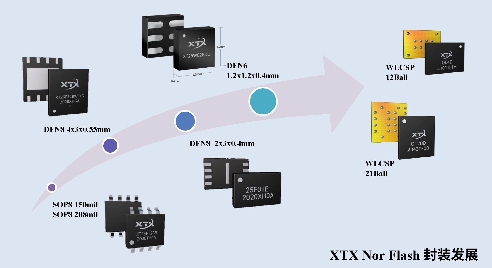
随着芯片封装技术的发展,半导体封装经历了从dip、sop等引脚插入式封装到dfn、bga等表面贴片封装再到wlcsp等晶片级封装的变革;同时随着智能穿戴等消费类电子产品的飞速发展,芯片封装技术面临着“集成度高、小型化、连接工艺升级”的挑战和机遇。
芯天下在面对市场机遇时适时推出了业内超小的dfn封装(1.2*1.2*0.4mm),同时在适配更先进封装技术的探索上未停下脚步。随着业内wlcsp封装技术的不断成熟,芯天下在2020年开始导入wlcsp的封装并已通过全面考核,将于2021年q1季度正式推出1.8v 64mb &128mb的wlcsp封装,后续会陆续推出全系列容量的wlcsp封装满足客户需求。
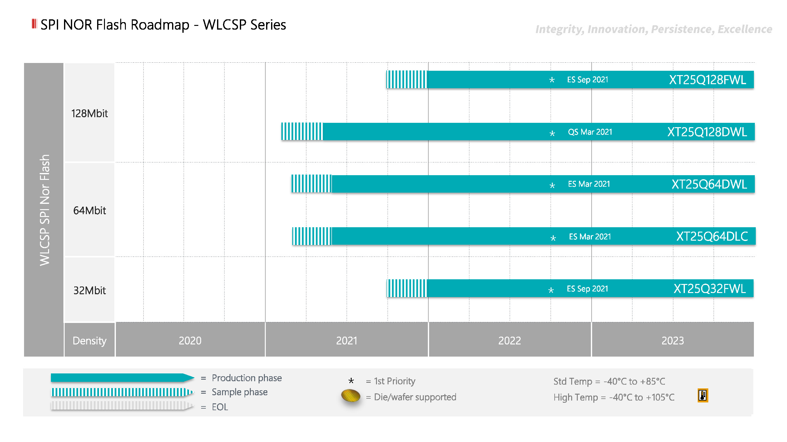
 芯天下wlcsp roadmap
 芯天下wlcsp 产品特点
wlcsp:wafer level chip scale packaging是晶片级芯片封装,是集成电路可实现的最小尺寸封装,其优点有:
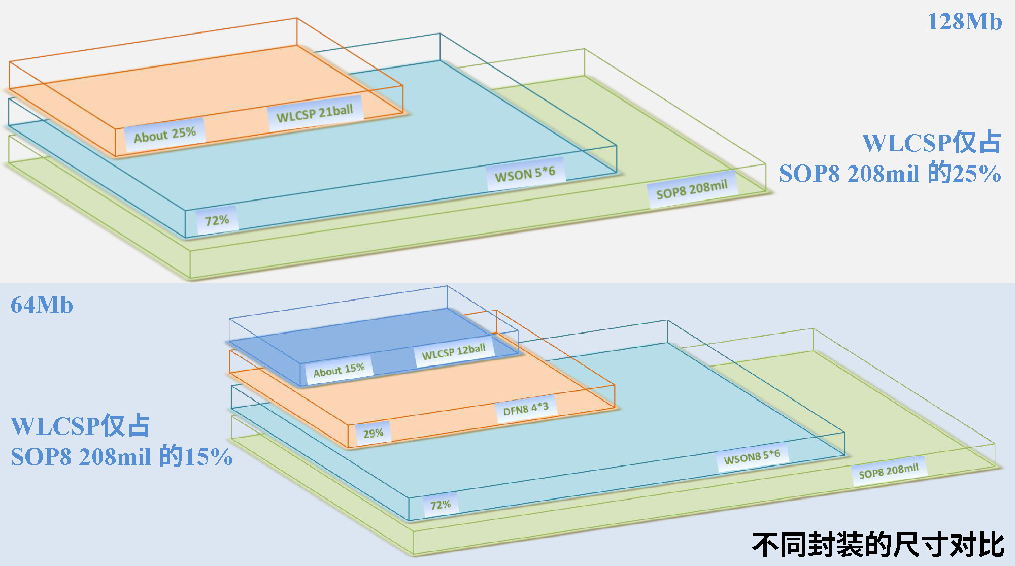
(1)外尺寸小:封装后的投影面积等同裸晶片的尺寸,做到封装尺寸和晶片尺寸1:1;
(2)电性能佳:相比传统打线,wlcsp内部引线短,信号完整性大幅度提高;
(3)可靠性好:无框架、注塑等引入的分层问题,散热性好。同时能够满足jedec msl-1(moisture sensitivity level-1)要求;
(4)兼容性强:兼容wlcsp业界标准封装,硬件上pin to pin替换。
|
产品型号
|
性能支持
|
|
xt25q64dwligt
xt25q64dlcigt
|
功能:
-
support advance sector/block protection
-
support standard/dual/quad spi
-
support spi/qpi mode
-
support dtr function
-
support 128mbit unique id
-
support output driver strength adjustable
性能:
-
deep power down current: 0.4ua
-
standby current: 12ua
-
page program time: 0.4ms typical
-
sector erase time: 40ms typical
-
block erase time: 0.12/0.15s typical
-
chip erase time: 40s typical
-
dual i/o data transfer up to 266mbits/s
-
quad i/o data transfer up to 532mbits/s
-
qpi mode data transfer up to 432mbits/s
-
dtr quad i/o data transfer up to 768mbits/s
|
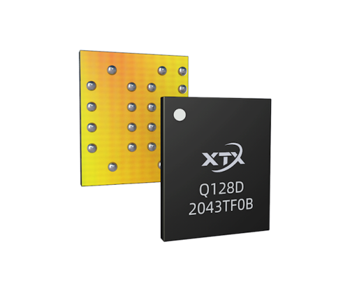
xt25q128dwligt
|
功能:
-
support advance sector/block protection
-
support standard/dual/quad spi
-
support spi/qpi mode
-
support dtr function
-
support 128mbit unique id
-
support output driver strength adjustable
性能:
-
deep power down current:0.4ua
-
standby current: 12ua
-
page program time: 0.4ms typical
-
sector erase time: 40ms typical
-
block erase time: 0.12/0.15s typical
-
chip erase time: 40s typical
|
应用实例
wlcsp的应用领域非常广泛,主要涉及智能穿戴,包括智能手表,手环,头戴式设备,tws等市场,例如:
1.智能眼镜
2.tws耳机
3.智能心率手环
量产支持
|
产品型号
|
封装
|
供货信息
|
xt25q64dwligt
xt25q64dlcigt
|
wlcsp 12 ball
wlcsp 12 ball
|
q2’21批量供应
|
|
xt25q128dwligt
|
wlcsp 21 ball
|
q2’21批量供应
|
凯发app的联系方式
获得现场支持&咨询,请您发送邮件至:;
获取销售支持&咨询,请您发送邮件至:sales@xtxtech.com;
获取更多产品信息,欢迎您访问芯天下凯发app官方网站官网:凯发app官方网站-凯发app。